Some use it a lot but not me, except maybe in
the crunch mode which is nice for the rythm guitar. But I said the Big
Lol GP2 guitar preamp is a versatile device so there is no way I coul
ommit the clean channel.
If you arrived here without having read the intro,
then you'd better go and have a look at it to know what's on here. Otherwise,
you just had so far some marketing-like description that everybody can
understand. From now, things gonna get tighter. Plug in the soldering iron
and while it's heating up, take a look at the schematic.
 Click on the picture for
more details on a block
Click on the picture for
more details on a block
According to the above block diagram, it seems
simple doesn't it but maybe some would appreciate a few details on each
stage to make clearer the connections between the boxes to the actual components
on the schematic.
 Input
buffer
Input
buffer
It is composed by IC1A and IC1B. The input impedance
is set to 470k by R8. If needed, it can be increased. A value of 1 meg
is fairly common. The gain is derived by (1 + R2/R3), that is (15dB). Q1,
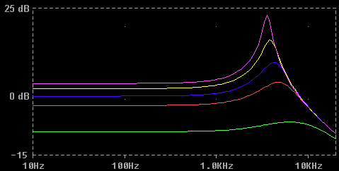
controlled by S1 switches on or off a high pass filter (bright)
that gives a 11dB boost at he high frequencies (see the bode plot below).
Note that Q1 switches an AC signal, what is not
academic at all. It may look bizarre but it works. However, don't ask me
exactly why, I wouldn't say. When S1 is open, the base of Q1 is reverse
biased (Vbe=-4V) so that the base collector junction is never direct biased,
even when the input signal is negative. If you think that this is much
too complex for the job it does, Q1 and its base circuit can be replaced
by a simple switch but you would loose the possibilty to control the bright
effect by a logic signal from a footswitch or why not, a midi interface.
IC1B is a classical op-amp based inverting amplifier
whose gain ranges from minus infinite (theoriticaly) to +20dB.
Bass
/ Trebble tone controls
Nothing more common than a traditionnal Baxendall filter built around IC2A.
High frequences are controlled by P3 and basses by P4. The frequency plot
is as below
Green, red and blue curves show the tone control frequency response for,
respectively, the min, middle and max position of the potentiometer P3
and P4. Unlike what is usually found in hi-fi systems, the mid position
does not lead to a flat response. This is due to the asymetry between R16
et R17 for the trebble and R15 et R18 for the bass. If you are not happy
with it, set R15 = R16 = R17 = R18 = 1k and it will be -theoritically-
perfectly flat but does anyone care ? Other smaller values may be used
to increase gain boost/cut and the capacitor values can be changed to modify
the cutoff frequencies. Try different values until your hears say they're
fine. Mine are happy with the values of the schematic.
Parametric
medium tone control
This circuit is the center piece of the tone control
section since it enables a very wide sound palette. It is made of
IC2B and IC3. Ok, I must admit that this eq is not fully parametric
but only semi-parametric, i.e. the bandwith/Q factor cannot be set. Nevertheless,
a parametric filter design is shown in the Big
Lol Output Filter section of the drive channel page. The plot below
shows the frequency response for min and max values of P1 (level) and for
values of P7 (frequency) varying with a 10k step. Clearly, the center
frequency does not vary linearly along with P7. This is whiy an antilog
pot (which may not be easy to find) should be prefered. See the notes
about it.
The Q factor (or bandwith) can be adjusted by modifying
the ratio C13/C33 and max boost/cut by modifying R45. The center frequency
range depends on the values of R24, R25 and P7.
Limiter
IC4A is the center piece of the crunch distorsion
of this channel. The nominal gain is set to 6db by the ratio R29/R33. The
distorsion effect is due to the switching diodes 1N4148
(or 1N914) that clip the signal. Try any diodes you may have in stock and
chose the ones that give the sound you prefer the most. A common trick
is to use different diode types to make the clipping asymetrical (who said
a Zener diode ?) and modify the harmonic content. Try also some LEDs (Marshall
does it) of various colors (i.e. various thresholds) : It looks nicer and
it may sound better. The final choice is up to you.
R30 allows to adjust the harshness of the distorsion.
Try different values or, if you have enough room on the front panel of
your rack, replace it by a potentiometer.
Lowpass
This filter uses the two op amps of IC7 and is in charge of attenuating
some dirty harmonics coming from the limiter while it boosts some others
since it's a resonant circuit. Actually, two filters are cascaded, all
this to make your ears comfortable.
IC7A is the center of a second order lowpass filter. It uses a de Sallen
& Key structure which is discussed everywhere in the litterature or
on the web. The bode plot of this filter is shown below.
The second filter is a twin T lowpass filter whose attenation is 6dB/oct
(see below).
The Q factor can be adjusted by P8. The green, red, blue, yellow and
purple plots have been obtained for P8 = 0, 22k, 47k, 100k and 220k
respectively. In my own guitar preamp, P8 is simply a adjustable resistor
since I had not enough space on the front panel but if you have some, you
definitely should make P8 a potentiometer. Some might say that it is nonsense
to use C42 and C43 (as well as R53 and R54) in parallel when a single 4.7nF
capacitor and a single 11k resistor would exactly the same. Definitely
wrong : If the Q factor is to be set by P8, then we absolutely need R53//R54
= R55/2 = R56/2 and C42//C43 = 2*C44 = 2*C45. Does somebody have a 4.4nF
capacitor ?
The overall filter has a 18 dB per octave slope as shown below.
The resonance frequency is about 3.5 kHz (2*pi*R55*C44)-1 and
the bandwith varies from 2.8 kHz to 4.5 kHz according to the value of P8.
Clean
/ crunch selection
This is here the first appearance of the Big Lol
Switching system, based on IC6, a CMOS 4053
(or CD4053, depending on the chip manufacturer)
analog multiplexer. The clean/crunch switch uses the X inputs (pins 12
et 13) of the circuit, and is controlled by a TTL compatible signal on
the A input (pin 11). If the control signal is low, the output signal (x
on pin 14) is equal to the one present at the input x0, i.e.the clean.
If the control signal is high, the output signal is the crunch signal (x1).
Le control signal comes from the logic module
(via J11) which enables to switch from clean to crunch (and back) either
from the control panel or from a footswitch or, if you want from the parallel
port of your PC.
The multiplexer is powered under +/- 7.5V because the max differential
voltage between VDD and VEE must not exceed 15V.
Those voltages are delivered by the transistors Q2 and Q3. Just in case,
D8 et D7 limit the clean signal excursion to a reasonable range, i.e. the
power voltages of IC6. This is useless to do the same with the crunch
signal since the limiter circuit has already done
it.
Volume
No explanation is needed here. The volume is set
by P6/IC4B and varies from minus infinite (still theoritically) to 0dB.
However, note that IC4B is also a output buffer for the effects loop and
that it allows to set the amplitude of the signal sent to the FX (J6).
Indeed, if most effects processors have an output volume, much fewer do
provide an input gain control.
Effects
loop
The FX loop circuit allows to insert (or not) an
effects processor. When an FX is inserted, the balance between the direct
signal (dry) and the signal coming from the FX (wet) on J7
can be adjusted by P5 (see below). As well as for the limiter, the FX loop
circuit uses the Big Lol Switching system
and the TTL control signal comes from the
logic module through J10.
As described before, the Send buffer relies
on IC4B. The ouput impedance is set by R37 to 220 Ohms. The Return
buffer lies in IC5A. Its input impedance is 68k (R39) and its gain
is unity.
The Send (dry) and Return (wet) signals are conected
via R40 and R41 to P5 whose whiper is grounded. R40 and P5 form a voltage
divider for the Dry signal and R41 and P5 do the same for the Wet
signal. Both dividers are controled by the same potentiometer P5. When
the whiper is in maximum position the Dry signal is grounded. Alternativey,
if the whiper is at minimum position, the Wet signal is grounded.
When the whiper is in the middle, the gains applied to the dry and
wet signals are the same. This allows to adjust the balance
between both signals when the loop is active, that is when an effect is
actually inserted.
The dry and wet signals, attenuated in proportions defined
by the mix (P5), are respectively sent to the inputs z1 and y1 of the multiplexer.
As for the clean/crunch selection circuit, D9 et
D10 limit the wet signal excursion so that it does not exceed the
power voltage of IC6. The dry signal is also sent to the inputs
y0 and z0 through R36.
IC5B is the output buffer of the channel. It adds (and inverts with
a 0dB gain) the signals from the ouputs y and z of the multiplexer. The
control inputs B and C are connected together. Therefore, depending of
the logic state of B and C, the signal at the ouput of IC5B is equal to
-(y0+zo) or -(y1+z1), i.e. dry (direct) or dry + wet
(mix).
If despite my efforts, the way this stage works is still not clear,
draw its schematic without IC6 in the two following cases.
1) B=C=0 => connect R42 and R43 to the pin 6 of IC4B
2) B=C=1 => connect R36 to the pin 6 de IC4B.
Much clearer ? Still not ? Don't bother, I swear it works just fine
!
The output connector J8 is aimed to provide a link with the channel
selector module. See the wiring section
for interconnecting modules. The output J9, via a coupling capacitor allows
to add a line level output for the clean channel.
Main
frame | Introduction | Clean channel | Drive
channel | Channel selector
Logic
module | Power supplies | Wiring
| Notes & Symbols | Schematics
| Demos | FAQ